2024-08-31 | [hp8x] [retrocomputing]
The HP 85A computer makes use of ROMS to add extra features. This not only includes software improvements, like support for matrix math, but also the 'drivers' for the hardware, like mass storage, plotters, or HP-IB.
The original roms were custom mask roms produced on a custom HP chip. They came as little plug in bricks you would insert into a ROM Drawer. You can't simply use an EPROM in place of one.
This sort of thing has been done before, of course. HP made the HP 82929A Programmable ROM which would let you use two 8K EPROMS to take the place of two ROM images. My design is heavily based around a reverse engineering project of the original HP card and a later reworking of that design into a PCB (at the bottom of curiousmarc's page).
There also is/was the PRM-85 project which is a FPGA design which does the same thing, except it has one EPROM chip with up to 8 images, instead of just two chips with one image each. I don't think the PRM-85 is as open source as the other projects, but it at least confirms that my approach is possible.
There is also the EBTKS Project which is a modern microcontroller based expansion card that can do the ROMs and much more. I have one and it's great. But I wanted a more hardware constrained solution also for just roms. If I'm going through the trouble to repair my tape drive, I feel as though I should at least attempt to be more on the side of period accuracy.
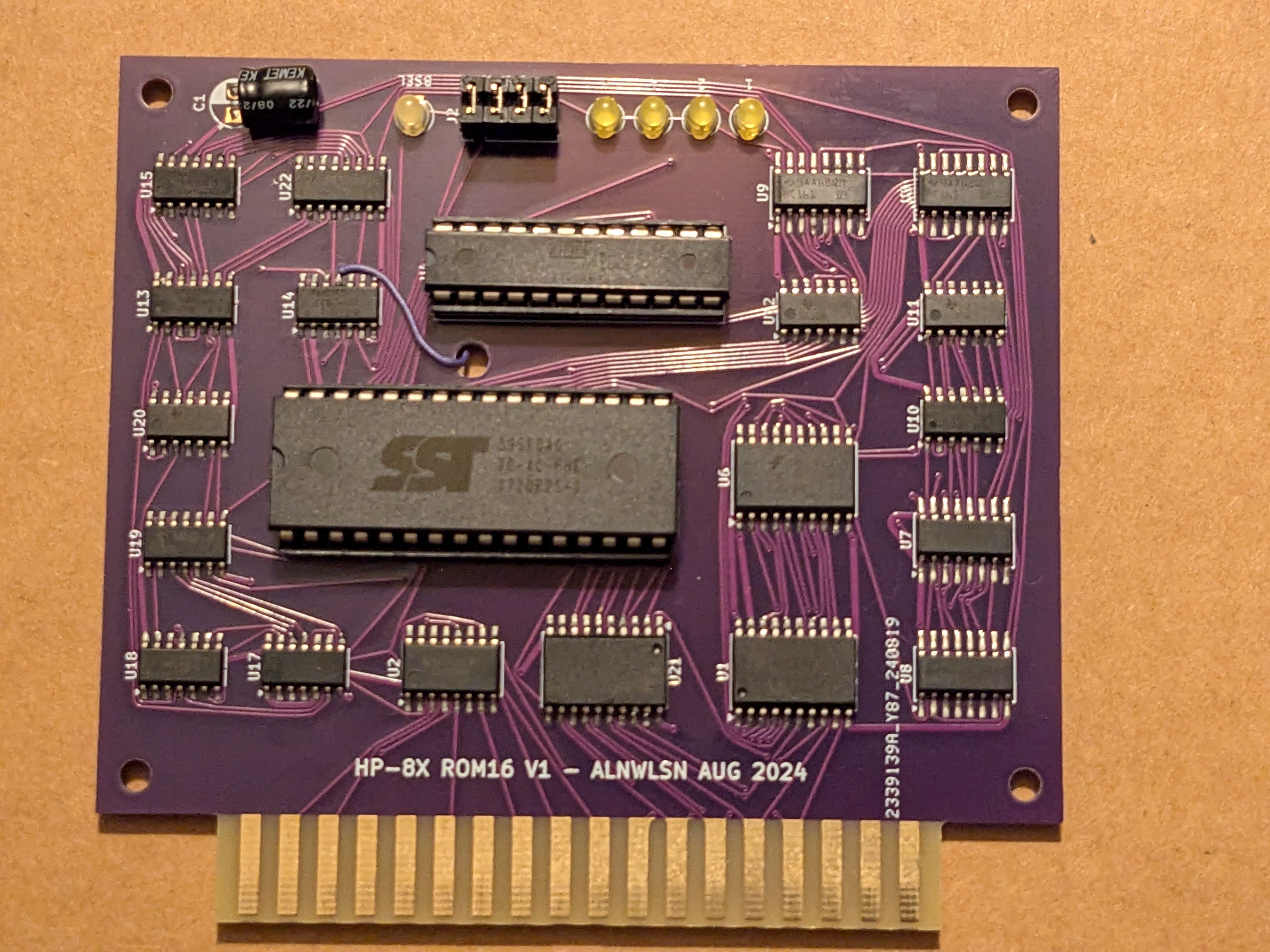
The original ROM drawer could hold 6 roms (actually, you could put in 2 rom drawers, or stack the physical rom chips on top of each other. So more than 6 could be used). For the HP 85, between hobby projects, official HP roms, and the service rom, there are about 10 roms available. I figured, for no reason apart from excess, to make mine to hold 16 roms.
To put 16 8K roms into a single chip, we'll need a 128K device, aka 1Mbit. That's a 27C1024 if it's an eprom. I usually stock 4M sized SST39SF040 flash roms for my Z80 projects, which are 4x bigger than I need, but share the same pinout as a 1M chip.
Each of the roms also has an associated ID, which is what slot the computer addresses the ROM from. The I/O rom needs to be in slot #192, and won't work in any other slot, for example. I used a PAL(GAL) chip for this; it does 2 things:
The rest of the circuitry is the same as the two 82929A clone projects, but with some of the extra gates cleaned up from not having the multiple eprom chips.
I also used mostly all 5V CMOS parts (74HC) since those were easier to get. The only thing not CMOS is the GAL, which feeds the flash chip, and the flash chip itself (which is a CMOS part but has TTL outputs). That makes the flash data lines feeding the CMOS input 74HC244 out of spec, but I assume that's why this clone has pull-up resistors on those lines. In any case, it works, so that's good enough in my book. The GAL also feeds the input to the 74 latch, so that one has to be an HCT part.
Translation of the rom IDs are done by changing this section in the source code for the PAL:
TABLE HPADR => EPROMADR  {
'b'00101000=>'b'0000; /* Assembler */
'b'10101000=>'b'0001; /* Forth */
'b'10110000=>'b'0010; /* Matrix */
'b'11000000=>'b'0011; /* I/O */
'b'11001111=>'b'0100; /* EMS */
'b'11010000=>'b'0101; /* Mass Storage */
'b'11010001=>'b'0110; /* Electronic Disk */
'b'11100000=>'b'0111; /* Service ROM */
'b'11101000=>'b'1000; /* Advanced Programming */
'b'11110000=>'b'1001; /* Printer/Plotter */
}
I compile this with WinCUPL which is free from Microchip. However, it's an old XP-era application, and is infuriating to use. While the compiler is fine, the interface feels only about 1/3 finished, and you're just a few button clicks away from total confusion. All you need to do is load the pld file, and then do device dependant compile. If it compiles without errors, the .JED file is ready to use.
Since there are a couple unused IO pins on the PAL, I used one to put in a disable for the Service Rom. If you leave the service rom in, the computer will boot into the service menu each time you turn it on.
I use the Chinese TL866II Plus, which is inexpensive for a parallel programmer, and works with both the flash chip and the modern Microchip ATF22V10CQZ PAL chip.
For the flash chip, all you need to do is concat all the 8K binary files together in the order that the translator sees them. For the source above, it would look something like this:
touch roms.bin
cat 85-assembler.bin >> roms.bin
cat 85-forth.bin >> roms.bin
cat 85-matrix.bin >> roms.bin
cat 85-io.bin >> roms.bin
cat 85-ems.bin >> roms.bin
cat 85-mass-storage.bin >> roms.bin
cat 85-electronic-disk.bin >> roms.bin
cat 85-service.bin >> roms.bin
cat 85-advanced.bin >> roms.bin
cat 85-printer.bin >> roms.bin
The completed roms.bin is what you load into the flash chip.
I made just one (electrical) mistake on my PCB, which was that the clock pin to latch the translated address to the flash chip is supposed to be connected on the clock line for the 74hc74 which latches the /BANKSEL signal, not on the output from that latch. The board download below has this trace corrected.